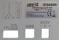
Joy-IT JDS6600
 | |
| Status | supported |
|---|---|
| Source code | juntek-jds6600 |
| Frequency (user) | 0-60MHz (sine), 0-15MHz (square, tri), 0-6MHz (PWM, arbitrary) |
| Waveforms | sine/square/triangle/arbitrary, TTL rect |
| Amplitude | not specified in the data sheet (UI claims -10V .. +10V) |
| Modulation | sweep, pulse, burst |
| Connectivity | USB/serial |
| Website | joy-it.net |
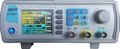
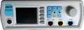
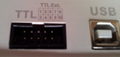
The JDS6600 is a dual channel, standalone function generator, and has builtin frequency measurement and pulse counter. There are push buttons and a rotary encoder on the front panel, the graphical LCD presents parameter values as well as waveforms. The rear panel has USB as well as UART connectivity, the device must be powered externally (not USB powered). Signals (external in, and generator out) get connected to BNC receptables, an IDC pin header provides TTL versions of these signals.
See Joy-IT JDS6600/Info for USB connection details.
Hardware (Joy-IT model 60MHz)
The PCB's contour seems to match the MHINSTEK MHS-5200A with three BNC receptables on the front, and the arrangement of the barrel jack, the USB B receptable, and the IDC pin header on the rear side. The lattice chip is identical. Earlier MHS revisions used the same CH340G USB chip before they switched to PL2303. MHS uses an STM8 controller while JDS uses STM32. That's about it. The analog stages differ vastly.
- FPGA: Lattice MACH XO2 1200HC TQFP-100 (marking: LCMX02-1200HC)
- MCU: GD(?) 32F103CBT6 (an OEM'ed version of the STM32 chip that is famously used in Bluepill boards?), 8MHz quartz
- Winbond 25Q16 SPI flash (2MiB, probably netlist, maybe UI resources(?), waveforms(?), settings(?))
- 74'14 inverters between FPGA and IDC pin header
- WCH CH340G USB to serial converter ("well known")
- R2R ladder connected to FPGA pins (two times 16 pins(?) for the two channels, some for the waveform outline, others for offset/gain control, coupling, enable, etc)
- LM358 for "DC use" (offset and gain control)
- most analog circuits have their top scrubbed off
- AD8xx chips, Youtube reviews and teardowns for MHS suggest AD603 (variable gain amplifier) and AD812, may be used here as well?
- two SO-8 chips each under two heatsinks (the output amplifiers?)
- output switch relays
- several 117 voltage regulators
- programming headers (pads) for the FPGA and the MCU
Photos
Front, device active, graphical user interface
Front cover, no BNC receptables to be seen (PCB removed)
Rear cover, no receptables (PCB removed), IDC pinout label
IDC pin header, BEWARE unusual pin numbering
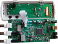
Two boards, taken out of the case
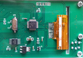
Front panel PCB, zoom on MCU and flash
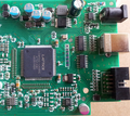
Digital part of main PCB: FPGA, R ladder, USB and IDC
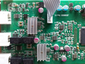
Analog part of main PCB: R ladder, offset, gain, amplifier and relays


Connection
The generator presents itself as a serial device (CH340G USB to serial converter, VID:PID is 1a86:7523, which is identical to MHS5200A).
Protocol
Serial communication is done at 115200/8n1 and carries text for requests and responses. Several end-of-line variants were seen in the field, LF and CR/LF are reported to work. Note that commands work when sent from programs, while interactive terminal sessions and slow typing may not be effective.
Requests take a form similar to ":w20=1,1.<crlf>" which translates to "write parameter 20" (the channels enabled state) while the multi-value right hand side enables CH1 and CH2 at the same time. There are "instruction codes" to write and read parameters, and to write and read arbitrary waveforms. Responses take a similar form for read commands, reflecting the parameter that was accessed when they provide its value(s). Write responses may just say ":ok<crlf>". It helps to think of the firmware's "register set" when dealing with read and write commands. Some values from the application's perspective are communicated in terms of multiple values on the wire. Think of frequency which gets expressed by means of an integer "mantissa" and a scaling factor's code(!). The factor itself is not seen on the wire, and many exchanges involve an implicit factor that neither is seen nor is it obvious either.
Resources
- Vendor's download area User manual (English, German), Software, Technical specifications
- Communication protocol as described by Joy-IT
- Kristoff Bonne github repo contains MIT licensed Python code for JDS6600 control
- EEVBlog forum thread on compatible devices