Difference between revisions of "Sysclk AX-Pro"
Jump to navigation
Jump to search
m (typo) |
|||
| Line 2: | Line 2: | ||
| image = [[File:SysCLK_AX_Pro_box.jpg|180px]] | | image = [[File:SysCLK_AX_Pro_box.jpg|180px]] | ||
| name = SysCLK USBee AX Pro clone | | name = SysCLK USBee AX Pro clone | ||
| status = | | status = supported | ||
| source_code_dir = fx2lafw | | source_code_dir = fx2lafw | ||
| channels = 8 | | channels = 8 | ||
Revision as of 02:37, 23 January 2014
 | |
| Status | supported |
|---|---|
| Source code | fx2lafw |
| Channels | 8 |
| Samplerate | 24MHz |
| Samplerate (state) | — |
| Triggers | none (SW-only) |
| Min/max voltage |
digital -1 to +6V |
| Threshold voltage | Fixed: VIH=1.6V, VIL=1.4V |
| Memory | none |
| Compression | none |
| Website | SysCLK |
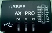
The SysCLK USBee AX Pro is a USB-based, 8-channel logic analyzer with up to 24MHz sampling rate, and with 2 additional analog channels. Analog channels are multiplexed by relay or solid-state IC to one ADC.
It is a clone of the CWAV USBee AX-Pro.
In sigrok, we use the open-source fx2lafw firmware for this logic analyzer.
Note: Only the logic analyzer functionality is supported so far, analog support is work in progress.
See SysCLK_AX-Pro/Info for some more details (such as lsusb -vvv output) on the device.
Hardware
- Main chip: Cypress CY7C68013A-56LTXC (FX2LP)
- I2C EEPROM: Atmel ATML125 24C02N SU27 D
- Auxillary 8051 chip: STC STC15F104E. Functional is unknown
- Supply voltage regulator: Advanced Monolithic Systems AMS1117-3.3
- Reference voltage regulator: Advanced Monolithic Systems AMS1117-2.851218
- Analog-to-Digital converter: Texas Instruments TLC5510I
- Analog input amplifiers: Analog Devices AD8065
- Analog amplifiers negative supply: Texas Instruments LMC7660
- Some operational amplifiers: Texas Instruments LM358
- Analog channel switching relay: TQ2-2V
- Crystal: 24MHz
- ...
FX2LP Pin mappings
| # | Pin | Destination | Remark |
|---|---|---|---|
| 01 | RDY0/SLRD | TRIG | socket pin |
| 13 | IFCLK | GND | grounded |
| 18..25 | PB0..7 | DCH0..7 | digital input |
| 30 | CTL1/FLAGB | CLK | socket pin |
| 31 | CTL2/FLAGC | ADC_CLK | ADC clock input |
| 33 | PA0 | relay | multiplexing ACH1/ACH2 |
| 35 | PA2 | DCH1 GND | can be isolated from GND and act as aux socket pin |
| 36 | PA3 | DCH2 GND | can be isolated from GND and act as aux socket pin |
| 38 | PA5 | STC_P3.1 | aux 8051 chip |
| 39 | PA6 | STC_P3.3 | aux 8051 chip |
| 42 | RESET# | STC_P3.2 | aux 8051 chip |
| 44 | WAKEUP | NC | not connected |
| 45..52 | PD0..7 | ADC_D1..8 | ADC data output |
Photos
Protocol
Since we use the open-source fx2lafw firmware for this device, we don't need to know the protocol.


