Difference between revisions of "YiXingDianZi MDSO"
(Added sigrok dump of eeprom communication with FX2 during booting.) |
Uwe Hermann (talk | contribs) (YiXingDianZi MDSO is now supported.) |
||
| (10 intermediate revisions by 2 users not shown) | |||
| Line 2: | Line 2: | ||
| image = [[File:YiXingDianZi-MDSO.png|180px]] | | image = [[File:YiXingDianZi-MDSO.png|180px]] | ||
| name = YiXingDianZi MDSO | | name = YiXingDianZi MDSO | ||
| status = | | status = supported | ||
| source_code_dir = | | source_code_dir = hantek-6xxx | ||
| channels = 2 | | channels = 2 | ||
| samplerate = 48MHz | | samplerate = 48MHz | ||
| Line 18: | Line 18: | ||
}} | }} | ||
The '''YiXingDianZi MDSO''' is a USB-based, 2-channel oscilloscope with an analog bandwidth of 20MS/s and 48MS/s sampling rate. | The '''YiXingDianZi MDSO''' (also known as '''Wosontel MDSO''') is a USB-based, 2-channel oscilloscope with an analog bandwidth of 20MS/s and 48MS/s sampling rate. | ||
It comes in very compact plastic case (82x65x23mm) without any branding | It comes in very compact plastic case (82x65x23mm) without any branding, USB type B input, 2c BNC inputs, and a red LED. | ||
See [[YiXingDianZi MDSO/Info]] for more details (such as '''lsusb -v''' output) on the device. | The YiXingDianZi manufacturer is probably the same as Instrustar (Chinese characters match, lsusb is almost exactly the same). | ||
See [[YiXingDianZi MDSO/Info]] for more details (such as '''lsusb -v''' output) on the device. | |||
== Hardware == | == Hardware == | ||
| Line 32: | Line 31: | ||
* ADC: Analog Devices AD9288 | * ADC: Analog Devices AD9288 | ||
* EEPROM: Microchip 24LC64I (64K I²C EEPROM) | * EEPROM: Microchip 24LC64I (64K I²C EEPROM) | ||
* 2x ST 74HC4051 (8-Channel | * 2x ST 74HC4051 (8-Channel analog mux) | ||
* Crystal oscillator 24MHz (crystal) | * Crystal oscillator 24MHz (crystal) | ||
* 4x 145 MHz FastFET | * 4x 145 MHz FastFET op amp: Analog Devices AD8065 (top markings HRA) | ||
* | * Unmarked DC/DC converter | ||
* 3.3V LDO: AMS1117-3.3 | * 3.3V LDO: AMS1117-3.3 | ||
| Line 42: | Line 41: | ||
<small> | <small> | ||
{{chip_56pin | {{chip_56pin | ||
| 1=PD5 | | 1=<span style="color:green">(AD9288 D5B)</span> PD5 | ||
| 2=PD6 | | 2=<span style="color:green">(AD9288 D6B)</span> PD6 | ||
| 3=PD7 | | 3=<span style="color:green">(AD9288 D7B)</span> PD7 | ||
| 4=GND | | 4=GND | ||
| 5=CLKOUT | | 5=CLKOUT | ||
| Line 62: | Line 61: | ||
| 18=VCC | | 18=VCC | ||
| 19=GND | | 19=GND | ||
| 20=<span style="color: | | 20=<span style="color:navy">(FX2 CTL0)</span> <span style="color:green">(AD9288 ENCA/B)</span> *IFCLK | ||
| 21=RESERVED | | 21=RESERVED | ||
| 22=<span style="color:purple">(EEPROM SCL)</span> SCL | | 22=<span style="color:purple">(EEPROM SCL)</span> SCL | ||
| 23=<span style="color:purple">(EEPROM SDA)</span> SDA | | 23=<span style="color:purple">(EEPROM SDA)</span> SDA | ||
| 24=VCC | | 24=VCC | ||
| 25=PB0 | | 25=<span style="color:green">(AD9288 D0A)</span> PB0 | ||
| 26=PB1 | | 26=<span style="color:green">(AD9288 D1A)</span> PB1 | ||
| 27=PB2 | | 27=<span style="color:green">(AD9288 D2A)</span> PB2 | ||
| 28=PB3 | | 28=<span style="color:green">(AD9288 D3A)</span> PB3 | ||
| 29=PB4 | | 29=PB4 <span style="color:green">(AD9288 D4A)</span> | ||
| 30=PB5 | | 30=PB5 <span style="color:green">(AD9288 D5A)</span> | ||
| 31=PB6 | | 31=PB6 <span style="color:green">(AD9288 D6A)</span> | ||
| 32=PB7 | | 32=PB7 <span style="color:green">(AD9288 D7A)</span> | ||
| 33=GND | | 33=GND | ||
| 34=VCC | | 34=VCC | ||
| 35=GND | | 35=GND | ||
| 36=CTL0 <span style="color: | | 36=CTL0 <span style="color:green">(AD9288 ENCA/B)</span> <span style="color:navy">(FX2 IFCLK)</span> | ||
| 37=CTL1 | | 37=CTL1 | ||
| 38=CTL2 | | 38=CTL2 | ||
| 39=VCC | | 39=VCC | ||
| 40=PA0 | | 40=PA0 | ||
| 41=PA1 | | 41=PA1 <span style="color:maroon">(CH1 74HC4051 S0)</span> | ||
| 42=PA2 | | 42=PA2 <span style="color:maroon">(CH1 74HC4051 S1)</span> | ||
| 43=PA3 | | 43=PA3 <span style="color:maroon">(CH1 74HC4051 S2)</span> | ||
| 44=PA4 | | 44=PA4 <span style="color:maroon">(CH2 74HC4051 S0)</span> | ||
| 45=PA5 | | 45=PA5 <span style="color:maroon">(CH2 74HC4051 S1)</span> | ||
| 46=PA6 | | 46=PA6 <span style="color:maroon">(CH2 74HC4051 S2)</span> | ||
| 47=PA7 | | 47=PA7 | ||
| 48=GND | | 48=GND | ||
| Line 96: | Line 95: | ||
| 50=VCC | | 50=VCC | ||
| 51=*WAKEUP | | 51=*WAKEUP | ||
| 52=PD0 | | 52=PD0 <span style="color:green">(AD9288 D0B)</span> | ||
| 53=PD1 | | 53=PD1 <span style="color:green">(AD9288 D1B)</span> | ||
| 54=PD2 | | 54=PD2 <span style="color:green">(AD9288 D2B)</span> | ||
| 55=PD3 | | 55=PD3 <span style="color:green">(AD9288 D3B)</span> | ||
| 56=PD4 | | 56=PD4 <span style="color:green">(AD9288 D4B)</span> | ||
}} | }} | ||
</small> | </small> | ||
''' | '''ST 74HC4051 (upper/lower, CH1/CH2) pinout''': | ||
<small> | <small> | ||
<table><tr><td> | <table><tr><th>CH1 (U13)</th><th>CH2 (U10)</th></tr> | ||
<tr><td> | |||
{{chip_16pin | {{chip_16pin | ||
|1=Y4 | |1=Y4 | ||
|2=Y6 | |2=Y6 | ||
|3=Z | |3=<span style="color:red">(AD8065 -in, via 1k to GND)</span> Z | ||
|4=Y7 | |4=Y7 | ||
|5=Y5 | |5=Y5 | ||
| Line 117: | Line 117: | ||
|7=VEE | |7=VEE | ||
|8=GND | |8=GND | ||
|9=S2 <span style="color: | |9=S2 <span style="color:blue">(FX2 PA3)</span> | ||
|10=S1 | |10=S1 <span style="color:blue">(FX2 PA2)</span> | ||
|11=S0 | |11=S0 <span style="color:blue">(FX2 PA1)</span> | ||
|12=Y3 | |12=Y3 <span style="color:red">(AD8065 out via 15k)</span> | ||
|13=Y0 | |13=Y0 <span style="color:red">(AD8065 out via 3.9k)</span> | ||
|14=Y1 | |14=Y1 <span style="color:red">(AD8065 out via 1k)</span> | ||
|15=Y2 | |15=Y2 <span style="color:red">(AD8065 out)</span> | ||
|16=VCC | |16=VCC | ||
}} | }} | ||
| Line 130: | Line 130: | ||
|1=Y4 | |1=Y4 | ||
|2=Y6 | |2=Y6 | ||
|3=Z | |3=<span style="color:red">(AD8065 -in, via 1k to GND)</span> Z | ||
|4=Y7 | |4=Y7 | ||
|5=Y5 | |5=Y5 | ||
| Line 136: | Line 136: | ||
|7=VEE | |7=VEE | ||
|8=GND | |8=GND | ||
|9=S2 <span style="color: | |9=S2 <span style="color:blue">(FX2 PA6)</span> | ||
|10=S1 | |10=S1 <span style="color:blue">(FX2 PA5)</span> | ||
|11=S0 | |11=S0 <span style="color:blue">(FX2 PA4)</span> | ||
|12=Y3 | |12=Y3 <span style="color:red">(AD8065 out via 15k)</span> | ||
|13=Y0 | |13=Y0 <span style="color:red">(AD8065 out via 3.9k)</span> | ||
|14=Y1 | |14=Y1 <span style="color:red">(AD8065 out via 1k)</span> | ||
|15=Y2 | |15=Y2 <span style="color:red">(AD8065 out)</span> | ||
|16=VCC | |16=VCC | ||
}} | }} | ||
</td></tr></table> | </td></tr></table> | ||
</small> | </small> | ||
'''Input stage gain''': | |||
{| border="0" style="font-size: smaller" class="alternategrey sortable sigroktable" | |||
|- | |||
!S2 | |||
!S1 | |||
!S0 | |||
!74HC4051D Mux | |||
!Gain | |||
!VDIVs | |||
|- | |||
| 0 || 0 || 0 || Y0 to Z (3.9k) || 5 (4.9 in fact) || 200mV | |||
|- | |||
| 0 || 0 || 1 || Y1 to Z (1k) || 2 || 500mV | |||
|- | |||
| 0 || 1 || 0 || Y2 to Z (0) || 1 || 1V | |||
|- | |||
| 0 || 1 || 1 || Y3 to Z (15k) || 16 || 62.5mV | |||
|} | |||
'''Microchip 24LC64I pinout''': | '''Microchip 24LC64I pinout''': | ||
| Line 162: | Line 180: | ||
</small> | </small> | ||
'''Analog Devices | '''Analog Devices AD9288 pinout''': | ||
{| border="0" style="font-size: smaller" class="alternategrey sortable sigroktable" | {| border="0" style="font-size: smaller" class="alternategrey sortable sigroktable" | ||
|- | |- | ||
| Line 222: | Line 240: | ||
| All-0xff. | | All-0xff. | ||
|} | |} | ||
== Photos == | == Photos == | ||
<gallery> | <gallery> | ||
File:YiXingDianZi-MDSO-box.jpg|<small>Packaging</small> | |||
File:YiXingDianZi-MDSO-outside.jpg|<small>Device, top</small> | |||
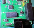
File:YiXingDianZi-MDSO-inside.jpg|<small>Inside</small> | |||
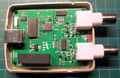
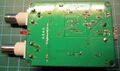
File:YiXingDianZi-MDSO-pcb-top.jpg|<small>PCB, top</small> | |||
File:YiXingDianZi-MDSO-bottom.jpg|<small>PCB, bottom</small> | |||
File:YiXingDianZi-MDSO-usb-side.jpg|<small>PCB, USB side</small> | |||
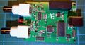
File:YiXingDianZi-MDSO-frontend.jpg|<small>PCB, analog frontend</small> | |||
</gallery> | </gallery> | ||
| Line 237: | Line 259: | ||
[[Category:Device]] | [[Category:Device]] | ||
[[Category:Oscilloscope]] | [[Category:Oscilloscope]] | ||
[[Category: | [[Category:Supported]] | ||
Latest revision as of 15:01, 28 December 2018
 | |
| Status | supported |
|---|---|
| Source code | hantek-6xxx |
| Channels | 2 |
| Samplerate | 48MHz |
| Analog bandwidth | 20MHz |
| Vertical resolution | 8bit |
| Triggers | none (SW-only) |
| Input impedance | 1MΩ‖25pF |
| Memory | none |
| Display | none |
| Connectivity | USB |
The YiXingDianZi MDSO (also known as Wosontel MDSO) is a USB-based, 2-channel oscilloscope with an analog bandwidth of 20MS/s and 48MS/s sampling rate.
It comes in very compact plastic case (82x65x23mm) without any branding, USB type B input, 2c BNC inputs, and a red LED.
The YiXingDianZi manufacturer is probably the same as Instrustar (Chinese characters match, lsusb is almost exactly the same).
See YiXingDianZi MDSO/Info for more details (such as lsusb -v output) on the device.
Hardware
- Cypress FX2LP CY7C68013A-56PVXC (USB 2.0 HS controller)
- ADC: Analog Devices AD9288
- EEPROM: Microchip 24LC64I (64K I²C EEPROM)
- 2x ST 74HC4051 (8-Channel analog mux)
- Crystal oscillator 24MHz (crystal)
- 4x 145 MHz FastFET op amp: Analog Devices AD8065 (top markings HRA)
- Unmarked DC/DC converter
- 3.3V LDO: AMS1117-3.3
Cypress FX2 pinout:
| (AD9288 D5B) PD5 | 1- | O | -56 | PD4 (AD9288 D4B) |
| (AD9288 D6B) PD6 | 2- | -55 | PD3 (AD9288 D3B) | |
| (AD9288 D7B) PD7 | 3- | -54 | PD2 (AD9288 D2B) | |
| GND | 4- | -53 | PD1 (AD9288 D1B) | |
| CLKOUT | 5- | -52 | PD0 (AD9288 D0B) | |
| VCC | 6- | -51 | *WAKEUP | |
| GND | 7- | -50 | VCC | |
| RDY0/*SLRD | 8- | -49 | RESET# | |
| RDY1/*SLWR | 9- | -48 | GND | |
| AVCC | 10- | -47 | PA7 | |
| (24MHz crystal) XTALOUT | 11- | -46 | PA6 (CH2 74HC4051 S2) | |
| (24MHz crystal) XTALIN | 12- | -45 | PA5 (CH2 74HC4051 S1) | |
| AGND | 13- | -44 | PA4 (CH2 74HC4051 S0) | |
| AVCC | 14- | -43 | PA3 (CH1 74HC4051 S2) | |
| (USB D+) DPLUS | 15- | -42 | PA2 (CH1 74HC4051 S1) | |
| (USB D-) DMINUS | 16- | -41 | PA1 (CH1 74HC4051 S0) | |
| AGND | 17- | -40 | PA0 | |
| VCC | 18- | -39 | VCC | |
| GND | 19- | -38 | CTL2 | |
| (FX2 CTL0) (AD9288 ENCA/B) *IFCLK | 20- | -37 | CTL1 | |
| RESERVED | 21- | -36 | CTL0 (AD9288 ENCA/B) (FX2 IFCLK) | |
| (EEPROM SCL) SCL | 22- | -35 | GND | |
| (EEPROM SDA) SDA | 23- | -34 | VCC | |
| VCC | 24- | -33 | GND | |
| (AD9288 D0A) PB0 | 25- | -32 | PB7 (AD9288 D7A) | |
| (AD9288 D1A) PB1 | 26- | -31 | PB6 (AD9288 D6A) | |
| (AD9288 D2A) PB2 | 27- | -30 | PB5 (AD9288 D5A) | |
| (AD9288 D3A) PB3 | 28- | -29 | PB4 (AD9288 D4A) |
ST 74HC4051 (upper/lower, CH1/CH2) pinout:
| CH1 (U13) | CH2 (U10) | ||||||||||||||||||||||||||||||||||||||||||||||||||||||||||||||||||
|---|---|---|---|---|---|---|---|---|---|---|---|---|---|---|---|---|---|---|---|---|---|---|---|---|---|---|---|---|---|---|---|---|---|---|---|---|---|---|---|---|---|---|---|---|---|---|---|---|---|---|---|---|---|---|---|---|---|---|---|---|---|---|---|---|---|---|---|
|
|
Input stage gain:
| S2 | S1 | S0 | 74HC4051D Mux | Gain | VDIVs |
|---|---|---|---|---|---|
| 0 | 0 | 0 | Y0 to Z (3.9k) | 5 (4.9 in fact) | 200mV |
| 0 | 0 | 1 | Y1 to Z (1k) | 2 | 500mV |
| 0 | 1 | 0 | Y2 to Z (0) | 1 | 1V |
| 0 | 1 | 1 | Y3 to Z (15k) | 16 | 62.5mV |
Microchip 24LC64I pinout:
| (VCC) A0 | 1- | O | -8 | VCC |
| (GND) A1 | 2- | -7 | WP (GND) | |
| (GND) A2 | 3- | -6 | SCL (FX2 SCL) | |
| VSS | 4- | -5 | SDA (FX2 SDA) |
Analog Devices AD9288 pinout:
| AD9288 pins | Description |
|---|---|
| S1, S2 | S1=VCC, S2=GND. "Normal operation, data align disabled". |
| DFS | Tied to GND. Data format select = "offset binary" (not "twos complement"). |
| AINA, AINB | Analog input channels. |
| D0A-D7A | Connected to FX2 PB0-PB7. |
| D0B-D7B | Connected to FX2 PD0-PD7. |
Firmware
Note: The firmware is flashed into the device permanently.
EEPROM layout
The device has a 8KB I²C EEPROM with the following layout:
c2 47 05 31 21 00 00 04 XX XX XX XX XX XX .. ..
Description:
| Bytes | Description |
|---|---|
| 0 | 0xc2: FX2 "c2 load" mode, i.e. VID/PID/DID are loaded from EEPROM as the firmware. |
| 1-2 | 0x0547: USB vendor ID (VID before firmware renumerate). |
| 3-4 | 0x2131: USB product ID (PID before firmware renumerate). |
| 5-6 | 0x0000: USB device ID (DID before firmware renumerate). |
| 7 | 0x04: FX2 configuration byte (see FX2 TRM for details). |
| 8-1917h | Firmware. |
| 1918h -1fffh | All-0xff. |
Photos
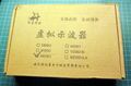
Packaging
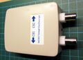
Device, top
Inside
PCB, top
PCB, bottom
PCB, USB side
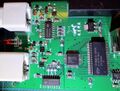
PCB, analog frontend


