Difference between revisions of "SainSmart DDS120"
Uwe Hermann (talk | contribs) (More info.) |
Uwe Hermann (talk | contribs) (Move vendor protocol info, cleanup firmware info.) |
||
| Line 62: | Line 62: | ||
== Protocol == | == Protocol == | ||
We use an open-source firmware that is part of [[fx2lafw|sigrok-firmware-fx2lafw]] for this device (i.e., not the vendor firmware/protocol), hence we do not need to know the vendor protocol. | |||
There is some [[SainSmart_DDS120/Info#Vendor_firmware|historic vendor firmware/protocol info]] for those interested, though. | |||
== Firmware == | == Firmware == | ||
The vendor firmware is contained on the I²C EEPROM. The FX2 boots directly into that firmware. However, we replace it (only in RAM, the EEPROM is never modified) with an open-source firmware that is part of [[fx2lafw|sigrok-firmware-fx2lafw]] when the device is attached to USB. | |||
The open source firmware is currently missing the following planned features: | |||
* <1MHz, 2, 3, 5, 6, 7.5, 9.6, 10, 15, 24, 30 MHz sampling rate support | * <1MHz, 2, 3, 5, 6, 7.5, 9.6, 10, 15, 24, 30 MHz sampling rate support | ||
| Line 102: | Line 80: | ||
The gain stage is 2 stage approach. -6dB and -20dB on the first stage (attentuator). The second stage is then doing the gain by 3 different resistor values switched into the feedback loop. The following does not correlate with measure on real hardware, there is a 6th gain position that is working though. It is very similar to another gain and was most likely omitted because of that. | The gain stage is 2 stage approach. -6dB and -20dB on the first stage (attentuator). The second stage is then doing the gain by 3 different resistor values switched into the feedback loop. The following does not correlate with measure on real hardware, there is a 6th gain position that is working though. It is very similar to another gain and was most likely omitted because of that. | ||
<small> | |||
# Channel 0: | # Channel 0: | ||
PC1=1; PC2=0; PC3= 0 -> Gain x0.1 = -20dB -> 0x02 (1V) | PC1=1; PC2=0; PC3= 0 -> Gain x0.1 = -20dB -> 0x02 (1V) | ||
| Line 117: | Line 96: | ||
PE1=0; PC4=0; PC5= 1 -> Gain x1 = 0dB -> 0x20 (0.100V) | PE1=0; PC4=0; PC5= 1 -> Gain x1 = 0dB -> 0x20 (0.100V) | ||
PE1=0; PC4=1; PC5= 0 -> Gain x2 = +6dB -> 0x10 (0.050V) | PE1=0; PC4=1; PC5= 0 -> Gain x2 = +6dB -> 0x10 (0.050V) | ||
</small> | |||
==== AC/DC coupling ==== | ==== AC/DC coupling ==== | ||
| Line 122: | Line 102: | ||
The coupling is controlled via 2 PhotoMOS chips. | The coupling is controlled via 2 PhotoMOS chips. | ||
<small> | |||
# Channel 0: | # Channel 0: | ||
PE3=0 Disable AC-coupling capacitor (DC- | PE3=0 Disable AC-coupling capacitor (DC-coupling) | ||
PE3=1 Enable AC-coupling capacitor | PE3=1 Enable AC-coupling capacitor | ||
# Channel 1: | # Channel 1: | ||
PE0=0 Disable AC-coupling capacitor (DC- | PE0=0 Disable AC-coupling capacitor (DC-coupling) | ||
PE0=1 Enable AC-coupling capacitor | PE0=1 Enable AC-coupling capacitor | ||
</small> | |||
==== 1kHz calibration square wave ==== | ==== 1kHz calibration square wave ==== | ||
Revision as of 21:20, 1 November 2016

The SainSmart DDS120 is a USB-based, 2-channel oscilloscope with an analog bandwidth of 20MS/s and 48MS/s sampling rate.
This device appears to be a rebadge of the Rocktech BM102 (or vice versa). The lsusb is exactly the same, the PCB is exactly the same (both have a "656517" and "102LJT1402" silkscreen), and the components used appear to be the same as well.
The device was apparently created by someone named "buudai" in 2012 (also reflected in the lsusb and in the former buudai.com website).
See SainSmart DDS120/Info for more details (such as lsusb -v output) about the device.
Hardware
- USB: Cypress CY7C68013A-100AXC (FX2LP) (datasheet)
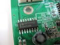
- 64-kbyte I²C EEPROM: Microchip 24LC64I (datasheet)
- Crystal: 24MHz
- 145 MHz FastFET Opamps: AD8065ART-R2: (datasheet)
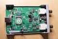
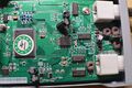
Or in newer hardware:
- Dual 8bit, 100MSPS ADC: MXTronix MXT2088 (datasheet)
- 145 MHz FastFET Opamps: AD8065: (datasheet)
- 4x CMOS differential 4-channel analog mux/demux with logic-level conversion: Texas Instruments CD4052B(M) (datasheet)
Photos
Teardown 1:
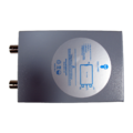
Device, top
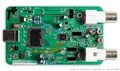
PCB, front
PCB, front
PCB, front
PCB, front
PCB, front
PCB, front
PCB, back
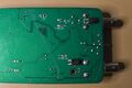
PCB, back
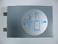
Box
Box
Box


Teardown 2 (purchased 03/2016):
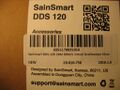
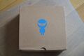
Sticker
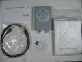
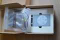
Package contents
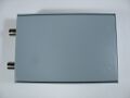
Device, top
Device, bottom
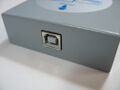
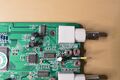
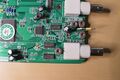
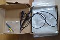
USB
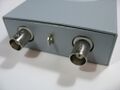
Connectors
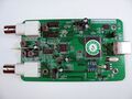
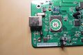
PCB, top
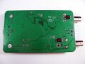
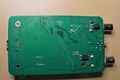
PCB, bottom
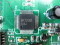
MXTronix MXT2088
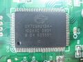
Cypress FX2
Microchip 24LC64I
TI CD4052BM
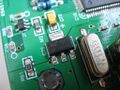
AMS1117-3.3
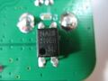
Unknown IC


Protocol
We use an open-source firmware that is part of sigrok-firmware-fx2lafw for this device (i.e., not the vendor firmware/protocol), hence we do not need to know the vendor protocol.
There is some historic vendor firmware/protocol info for those interested, though.
Firmware
The vendor firmware is contained on the I²C EEPROM. The FX2 boots directly into that firmware. However, we replace it (only in RAM, the EEPROM is never modified) with an open-source firmware that is part of sigrok-firmware-fx2lafw when the device is attached to USB.
The open source firmware is currently missing the following planned features:
- <1MHz, 2, 3, 5, 6, 7.5, 9.6, 10, 15, 24, 30 MHz sampling rate support
- Turn on/off the calibration pulse
- Change frequency of the calibration pulse (add 10kHz, 100kHz and 1MHz)
Gain stage
The gain stage is 2 stage approach. -6dB and -20dB on the first stage (attentuator). The second stage is then doing the gain by 3 different resistor values switched into the feedback loop. The following does not correlate with measure on real hardware, there is a 6th gain position that is working though. It is very similar to another gain and was most likely omitted because of that.
# Channel 0:
PC1=1; PC2=0; PC3= 0 -> Gain x0.1 = -20dB -> 0x02 (1V)
PC1=1; PC2=0; PC3= 1 -> Gain x0.2 = -14dB -> 0x0A (0.5V)
PC1=1; PC2=1; PC3= 0 -> Gain x0.4 =  -8dB -> 0x06 (0.250V)
PC1=0; PC2=0; PC3= 0 -> Gain x0.5 =  -6dB -> 0x00 (0.200V)
PC1=0; PC2=0; PC3= 1 -> Gain x1   =   0dB -> 0x08 (0.100V)
PC1=0; PC2=1; PC3= 0 -> Gain x2   =  +6dB -> 0x04 (0.050V)

# Channel 1:
PE1=1; PC4=0; PC5= 0 -> Gain x0.1 = -20dB -> 0x02 (1V)
PE1=1; PC4=0; PC5= 1 -> Gain x0.2 = -14dB -> 0x22 (0.5V)
PE1=1; PC4=1; PC5= 0 -> Gain x0.4 =  -8dB -> 0x12 (0.250V)
PE1=0; PC4=0; PC5= 0 -> Gain x0.5 =  -6dB -> 0x00 (0.200V)
PE1=0; PC4=0; PC5= 1 -> Gain x1   =   0dB -> 0x20 (0.100V)
PE1=0; PC4=1; PC5= 0 -> Gain x2   =  +6dB -> 0x10 (0.050V)
AC/DC coupling
The coupling is controlled via 2 PhotoMOS chips.
# Channel 0:
PE3=0 Disable AC-coupling capacitor (DC-coupling)
PE3=1 Enable AC-coupling capacitor

# Channel 1:
PE0=0 Disable AC-coupling capacitor (DC-coupling)
PE0=1 Enable AC-coupling capacitor
1kHz calibration square wave
Pin PE2 controls the frequency of the calibration output on the PCB. It is driven by an ISR timer from the 8051 core of the FX2 chip.