Difference between revisions of "Kingst LA2016"
| Line 76: | Line 76: | ||
Datasheets | Datasheets: | ||
U15 [http://www.ti.com/lit/ds/symlink/tps60403.pdf TPS60403] Charge pump voltage inverter | U15 [http://www.ti.com/lit/ds/symlink/tps60403.pdf TPS60403] Charge pump voltage inverter | ||
Revision as of 14:17, 5 March 2021
 | |
| Status | in progress |
|---|---|
| Source code | kingst-la2016 |
| Channels | 16 |
| Samplerate | 200MHz max. |
| Samplerate (state) | State analysis not supported |
| Triggers |
Level (multiple channels) Edge (one channel) |
| Min/max voltage | -50V — 50V |
| Threshold voltage |
Configurable: -4V—4V, min step 0.01V |
| Memory |
128MByte DDR2 SDRAM 40M—10G samples |
| Compression | Yes |
| Website | qdkingst.com |
5th March 2021:
This device was previously marked as supported, however, some users are reporting issues with this device and we are working on some driver changes.
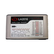
The Kingst LA2016 is a USB-based, 16-channel logic analyser with 200MHz maximum sampling rate.
The current vendor is "Qingdao Kingst Electronics Co., Ltd." but older models appear to be branded "Jiankun" rather than "Kingst".
The vendor software can be freely downloaded from their website.
Hardware
This logic analyser has been on the market since around 2012 and there are a few different revisions of it. This schematic has been reverse engineered from a unit purchased in 2020 containing a PCB marked as v1.3.0. The circuitry of early issue PCBs is similar but may have different voltage regulators, different input channel routing to the FPGA and no input threshold adjustment.
The LA1016 uses identical hardware with a different FPGA bitstream which limits the sample rate to 100MHz maximum.
All of these devices use the same firmware for the FX2LP MCU but there are four different FPGA bitstreams; i.e. LA1016 & LA2016 bitstreams and the older versions of these (to swap some of the input channels). Once the FX2LP firmware has been loaded, a 'magic number' is read from EEPROM which identifies the device and thus allows the correct FPGA bitstream to be loaded.
Note that the LA1016 cannot be boosted to 200MHz by changing the 'magic number' or the FPGA bitstream because of device U10 which is used by the FPGA to authenticate the bitstream. It is also used by the OEM software to authenticate the logic analyser as genuine 'Kingst'. U10 does not impact Sigrok support in any way and we don't need to communicate with it.
Main components and their function:
- Cypress FX2LP MCU
- This MCU only has volatile memory and in this implementation it's firmware is loaded from the host by the application software.
- Either the OEM firmware or open source firmware can be used.
- In essence, it just performs data moving operations:
- Endpoint 0 to EEPROM read/write
- Endpoint 0 to SPI read/write for FPGA control registers
- Endpoint 2 bulk out to SPI for loading FPGA bitstream
- Endpoint 6 bulk in to read capture data from FPGA/SDRAM
- Atmel AT24C02 2Kbit EEPROM
- This non-volatile memory stores:
- VID:PID which is 77a1:01a2 for LA1016 and LA2016 devices.
- 'magic number' to identify model and revision
- purchase date (presumably for warranty claims)
- other information related to U10 but not of interest to Sigrok
- Altera EP4CE6 FPGA
- Currently uses the OEM bitstream.
- Has a bank of approximately 60 byte-wide registers accessed via SPI which are used to contol FPGA functions.
- Captures 16 input channels, performs compression (run length encoding, 16bit sample plus 8 bit repetition count).
- Stores samples to SDRAM (or streams direct to USB but we don't implement that method).
- Interestingly, this device (6K LE) shares the same die as the next up device EP4CE10 (10K LE) and can be programmed as such. However, functionality would not be guaranteed as CE6 devices may be CE10 rejects.
- Samsung DDR2 SDRAM
- Samples are stored as 3 bytes (16bit sample plus 8 bit repetition count)
- A 'transfer packet' for upload is 16 bytes = 5 compressed samples plus a sequence number byte
- Burst read/write for this SDRAM is up to 16 bytes, which matches the transfer packet size and is likely used for all SDRAM read/writes.
Datasheets:
U15 TPS60403 Charge pump voltage inverter
Photos
Firmware
TODO This extraction script needs updated
In order to use this device you need to extract the firmware/FPGA files from the vendor software (Linux download) using the sigrok-fwextract-kingst-la2016 script from the sigrok-util repo and place them in one of the usual places where libsigrok expects firmware files:
$ ./sigrok-fwextract-kingst-la2016 KingstVIS/KingstVIS
saved 180224 bytes to kingst-la2016a-fpga.bitstream
saved 5350 bytes to kingst-la-01a1.fw
saved 5430 bytes to kingst-la-01a2.fw
saved 5718 bytes to kingst-la-01a3.fw
saved 142412 bytes to kingst-la-01a4.fw
saved 5452 bytes to kingst-la-03a1.fw


